Typical application circuit of capacitor mainly include filter circuits, phase shift circuits, coupling circuits, voltage divider circuits, etc.
(1) Mains filter circuit
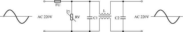
The mains filter circuit in a typical application circuit of capacitor is shown in Figure 1-1. C1 and C2 connected in parallel with the mains input circuit are high-frequency filter capacitors. They and the transformer L can filter out high-frequency interference pulses in the mains grid, and can also filter out high-frequency interference pulses generated by the circuit to avoid channeling. Access to the city power grid affects the normal operation of other power-using equipment. In general, the larger the capacitance, the better the filtering effect on the interference pulses in the mains. However, since the larger the capacitance, the smaller the capacitive reactance, and the greater the power consumption, so a capacitor with too large a capacity cannot be used as the mains filter capacitor.
prompt
Since the capacitor also has a certain hindrance to the passing of alternating current, the hindrance is called “capacitive reactance”. Therefore, the capacitance reactance of the capacitor is sometimes understood as a special resistance when analyzing the circuit. The size of the capacitive reactance is inversely proportional to the size of the capacitor and the frequency of the alternating current, that is, the higher the frequency, the smaller the capacitive reactance, and the larger the capacity, the smaller the capacitive reactance.
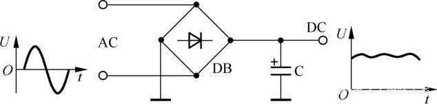
(2) DC voltage filter circuit
The DC voltage filter circuit in a typical application circuit of capacitor is shown in Figure 1-2. The core components of the circuit are the rectifier stack DB and the filter capacitor C. The AC voltage is rectified by the DB bridge, and the DC voltage is generated after filtering with C.
prompt
The larger the capacity of C, the better the filtering effect and the purer the DC voltage. However, the larger the capacitance of the same specification, the higher the price. Therefore, in the case of ensuring the normal operation of the circuit, it is sufficient to select a capacitor with an appropriate capacity.
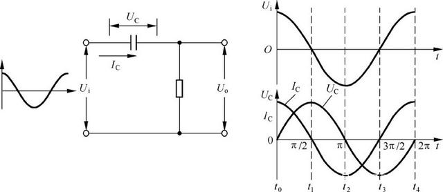
(3) Mains phase shift function of capacitor
Because the capacitor has the characteristics that the current can be abrupt and the voltage cannot be abrupt, the current through the capacitor will lead the voltage across it by 90 °, as shown in Figure 1-3.
(4) Capacitive coupling circuit
The capacitive coupling circuit in a typical application circuit of capacitor is shown in Figure 1-4. VT1 and VT2 in this circuit are amplifier tubes, C1-C3 are low-frequency signal coupling capacitors, and U i is an input signal.
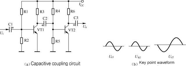
U i is coupled to the base of the amplifying tube VT1 through C1. After its inverting amplification, it is then coupled to the base of VT2 using C2, and then amplified again using VT2. The AC output signal U o is obtained through the coupling of C2. C1 isolates the DC voltage on the base of VT1 from the signal source, and C2 isolates the high DC potential of the collector of VT1 from the low potential of the base of VT2, but they are almost wires for low-frequency AC signals, so low-frequency signals can be Passed smoothly and amplified by the amplifier.
prompt
Since the capacitor has the characteristics of blocking DC and passing AC, the signal waveforms of the input and output terminals of C1 to C3 are the same, that is, the phase and frequency of the AC signal coupled through the capacitor are unchanged.
note
Since the coupling capacitors used in the low-frequency signal amplification circuit are mostly polar electrolytic capacitors, pay attention to the polarity of the capacitor when installing. The positive electrode must be installed on the side with high potential, otherwise the capacitor may be damaged, such as the positive electrode of C2. The collector of VT1.
(5) Voltage divider circuit
Figure 1-5 shows a partial circuit of a typical CRT large-screen color TV line output circuit. The core components of this circuit are filter capacitors C1 and C2. Due to the capacitive reactance of the capacitor, the voltage divider circuit composed of C1 and C2 not only divides the line reverse pulse, but also divides the DC voltage B +.
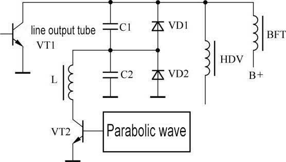
Changing the magnitude of the DC component of the field-frequency parabolic wave can change the degree of conduction of VT2, which also changes the level of the DC voltage at both ends of C2, and finally changes the magnitude of the deflection current flowing through the HDV deflection yoke to achieve horizontal amplitude adjustment. When adjusting the amplitude of the field frequency parabolic wave, by changing the amplitude of the waveform at both ends of C2 and the amplitude of the field frequency parabolic wave applied to both ends of C2, the horizontal pincushion distortion can be corrected finally.