A GPU sitting idle draws a fraction of what it draws one clock later. On a Blackwell-class accelerator running at roughly 1000 W, the core rail sits near 0.85 to 0.9 V while the current swings across several hundred amperes as tensor cores spin up. The regulator cannot follow that edge. It is far from the die, and its control loop is slower than the load.
What holds the rail up in the gap is capacitance. Deciding where that capacitance goes means splitting the load step into time zones, because each zone has a different dominant parasitic and a different way of failing when under-provisioned.
For the wider picture of how capacitor families divide work across an AI server power chain, the four-capacitor overview runs the rail from 380 V down to 1 V. This piece stays on one rail and goes deep.
A load step outruns the regulator
Take a boost converter feeding a GPU core rail. A workload transition pushes demand from 200 A to 600 A in a few hundred nanoseconds. The VRM senses the droop, its error amplifier responds, the inductor current ramps. Between the demand and the delivery, something has to hold the rail.
How far it may sag is a design decision rather than a datasheet constant. Most accelerator designs work to two to five percent around nominal. On a 0.9 V rail, three percent is 27 mV. That number drives every sizing decision below.
Target impedance sizes the array
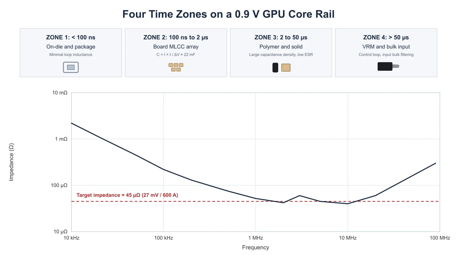
Convert the window into a specification with target impedance:
Ztarget = ΔVallowed / ΔIstep
At 27 mV and a 600 A step, the PDN has to look like 45 µΩ or less wherever the step has energy.
Forty-five micro-ohms is hard to reach with discrete parts. One 1210 MLCC has ESR in the low milliohms and ESL near 1 nH, and its own impedance bottoms out well above the target. The array works because many parts in parallel divide both, and because the parts are spread across frequency. Layering gets the curve under the line. A single large capacitor does not, which is the whole reason the array exists.
Four time zones on one rail
Planning a GPU decoupling array by time rather than by capacitance value keeps the parasitics honest.
Below 100 ns: inside the package
In the first tens of nanoseconds the current loop never leaves the die and its package. On-chip capacitance and the substrate planes supply the charge. Board capacitors are excluded by the inductance of the path between them and the die.
Package and interposer design get so much attention for this reason. Nothing soldered to the PCB changes what happens here. Vertical power delivery, with the regulator underneath the die rather than beside it, exists mostly to shorten this loop.
100 ns to 2 µs: the board MLCC array
Once the demand outlives the package, the board array takes over. Most of the capacitor count lives in this band, and most of the design arguments happen here. Ceramic parts win on ESL and ESR, and they can sit within a few millimetres of the die.
Two numbers drive the count: the charge the array must hold, and the parallel impedance it must present. The charge figure is easy to underestimate. Supplying 600 A for one microsecond moves 600 microcoulombs, and holding a 27 mV window while doing it takes roughly 22 mF at the die:
C = I × t / ΔV = 600 A × 1 µs / 27 mV ≈ 22 mF
Twenty-two millifarads in ceramic means more than 700 pieces of 1210 at an effective 30 µF each, on one rail. Nobody builds that. The arithmetic earns its place by showing how the job actually splits: regulator bandwidth shortens the window, and the array covers whatever remains. Treat the bank as the sole energy source and the board stops routing.
2 to 50 µs: polymer and solid electrolytics
Past a couple of microseconds the regulator is awake and the inductor current is climbing, though the loop is still catching up. Polymer tantalum and solid aluminum parts work in this band. They carry far more capacitance per unit area than ceramic, they take the ripple current, and their ESR is low enough to matter at these lower frequencies.
Misplacing parts between this band and the ceramic band is common. A polymer part where ceramic belongs adds bulk without lowering the high-frequency impedance. Ceramic where bulk belongs leaves the low-frequency end unsupported, which shows up as a slow sag under sustained load rather than a fast transient.
Above 50 µs: the regulator and its bulk input
At millisecond scale the VRM is in control. What remains downstream is bulk capacitance that rides through input transients and keeps the regulator’s own supply steady. Aluminum electrolytics still do that work on the input side, picked for capacitance per dollar and ripple handling rather than speed.
You get less capacitance than you order
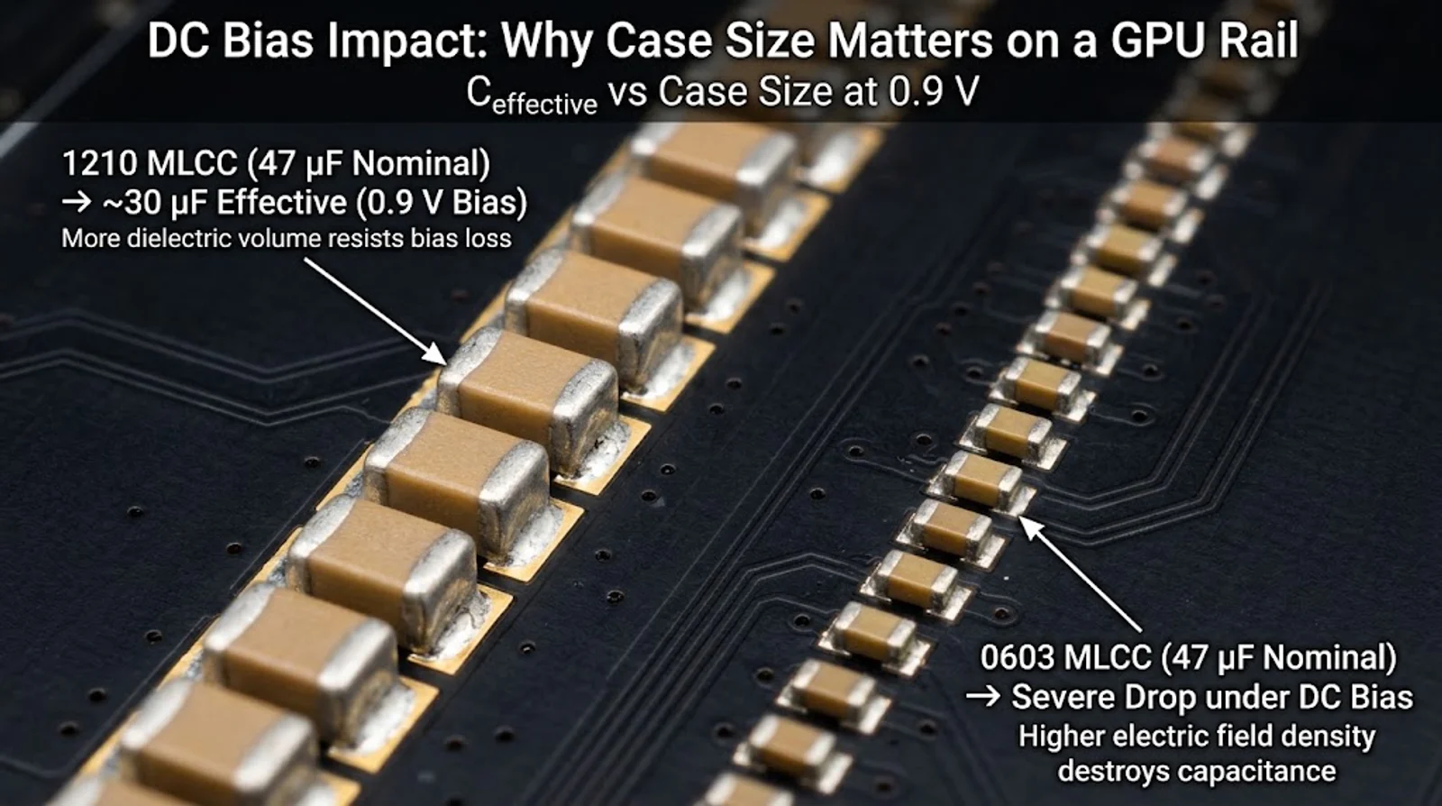
A BOM that says 47 µF and an impedance curve that behaves like 30 µF is ordinary on a low-voltage rail. On a 0.9 V GPU rail, DC bias does most of the damage.
DC bias on Class II ceramic
Class II dielectrics such as X5R and X7R use barium titanate, and its permittivity falls as the applied field rises. This is the material behaving as specified, not a bad batch. Published curves show small-case parts losing over half their nominal value at a few volts, and losses past 80 percent are recorded for high-capacitance-density parts running inside their ratings.
Case size changes the shape of the curve. More dielectric volume per unit capacitance, as in a 1210 rather than an 0603, usually holds value better at the same voltage. Board area is tight on accelerator cards, and large case sizes survive anyway for this reason.
At 0.9 V the applied field stays far from the rating, so bias derating is milder there than it would be at 5 V. The trap sits on the 48 V intermediate bus and the 12 V rails feeding the regulators, where a part chosen by a blanket fifty percent voltage rule can lose most of its value. Read the bias curve for the exact part number and case size.
Ageing and temperature drift
Class II ceramics also lose capacitance with time after the last heat treatment, and recover on reflow. The drift is logarithmic and flattens, so a part measured on the bench and the same part measured a year later on a card differ by several percent. Temperature adds another shift on top. Neither moves the design as much as bias, and both explain why field measurements rarely match the BOM.
The anti-resonance peak nobody budgets for
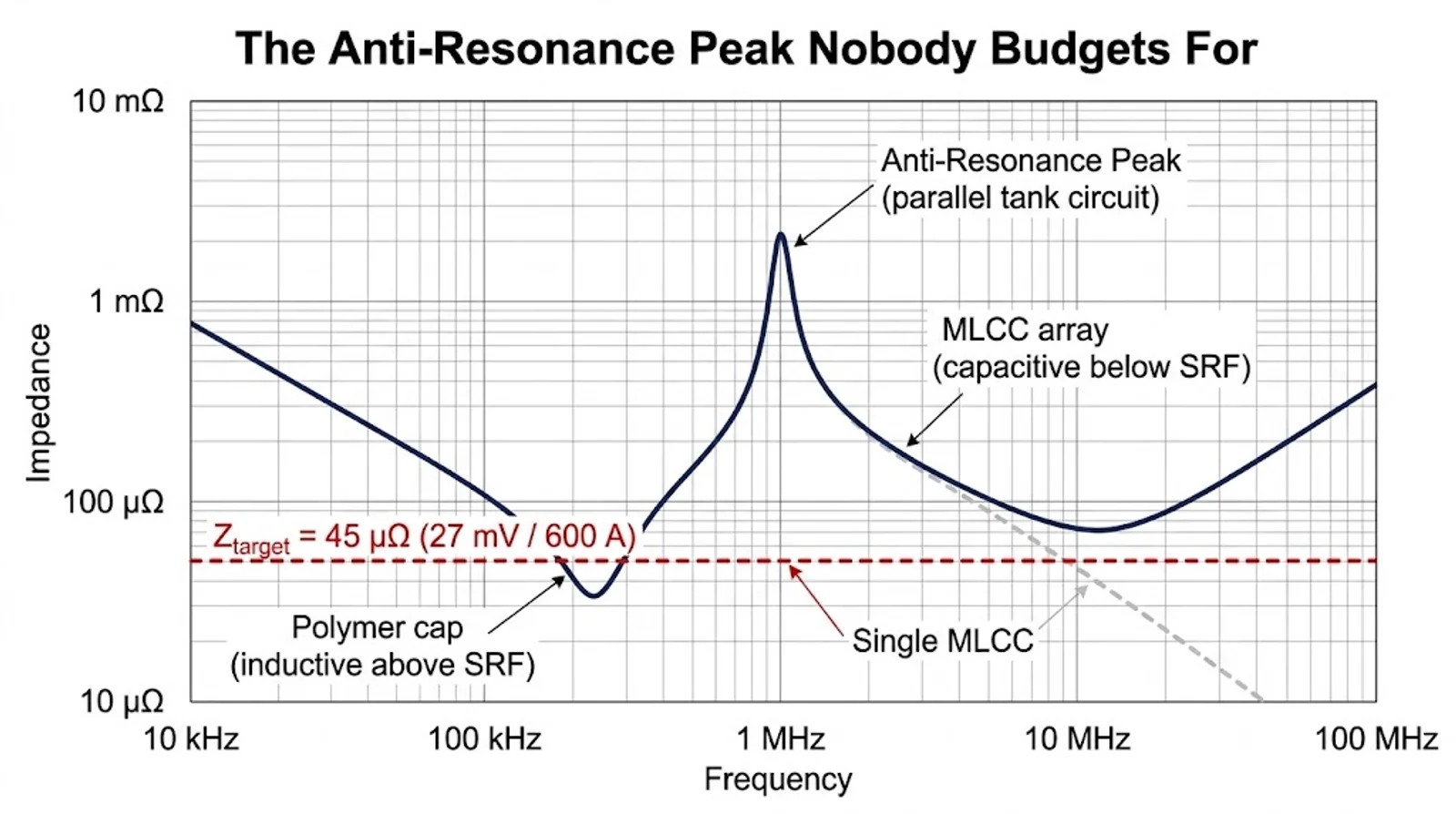
Mixing capacitor values sounds like it broadens the impedance curve. It creates a peak instead.
Between the two self-resonant frequencies, the larger capacitance has turned inductive while the smaller one is still capacitive. In parallel they behave like a tank circuit, and impedance climbs at the frequency where that happens. A PDN can pass its target at low frequency, look clean at high frequency, and miss in the band between. If the load current has harmonic content there, the rail sees more noise than the average figure suggests.
Keeping the spread between neighbouring values modest helps, and so does using many parts of one value rather than a wide ladder. Where a peak cannot be avoided, add damping. Simulation is the only reliable check, because the peak position depends on layout parasitics rather than on the capacitor list.
Choosing the mix
Below is a starting point for a GPU rail in the 500 to 1000 A class. The values reflect what the time zones call for, not a prescription for any particular board.
| Time zone | Dominant part | What decides the choice | Common error |
|---|---|---|---|
| < 100 ns | On-die and package capacitance | Package and interposer design, not BOM | Assuming board parts can fix a package loop |
| 100 ns to 2 µs | MLCC, 0402 to 1210, Class II | Bias derating, ESL, placement distance | Counting nominal capacitance in the BOM |
| 2 to 50 µs | Polymer tantalum, solid aluminum | Capacitance density, ripple rating | Placing polymer where ceramic is needed |
| > 50 µs | Aluminum electrolytic on the input | Ripple current, life at operating temperature | Sizing only for capacitance and ignoring life |
For the rail-by-rail version of this table, including the 380 V bus and the 48 V intermediate stage, the selection guide for AI server power stages covers the same ground with the regulator topology included. If the term itself is new, the decoupling capacitor basics page starts further back.
What changes at 1000 W
Current density comes first. A card at 1000 W on a 0.9 V core rail pushes more than a thousand amperes through a plane, and resistive drop across that plane stops being a second-order concern. Copper thickness, via count and the number of parallel layers all move into the budget.
Space moves the other way. Capacitor count grows while the footprint beside the die shrinks, and accelerator boards are already crowded with decoupling. That pressure is what pushed vertical power delivery from a research idea into shipping products.
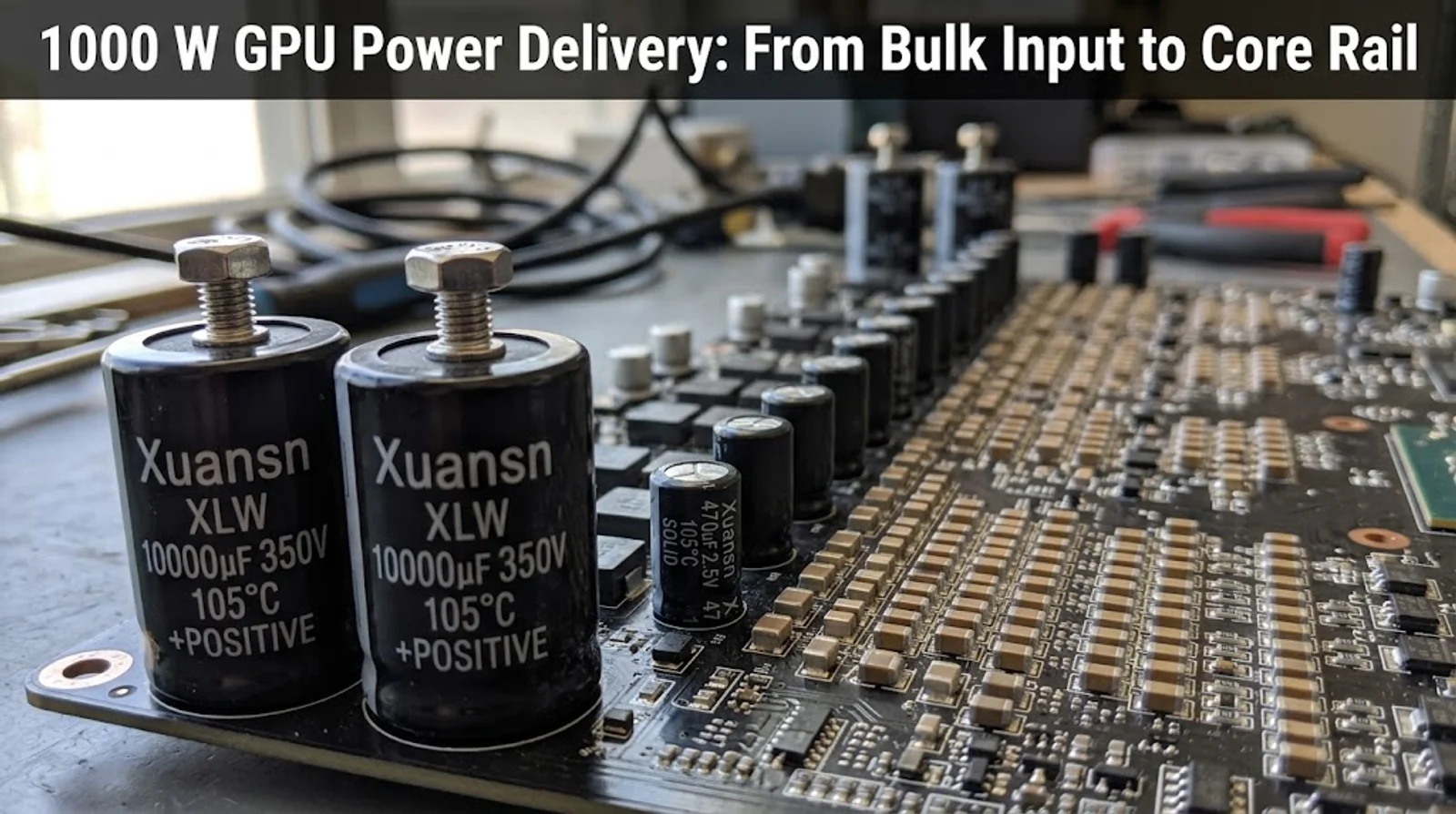
For the capacitor supply chain both trends point one direction. Demand shifts toward low-ESR, high-reliability parts in small cases, and toward polymer and solid types that hold their ratings under heat. Sourcing them at consistent quality is the less glamorous half of the problem. Xuansn builds aluminum electrolytic, film, solid and supercapacitor lines to customer specification, and the ceramic and solid ranges are catalogued under the multilayer ceramic and solid capacitor categories.
Where this sits in the AI power series
This is the GPU power rail installment of a series that began with why AI server power demand is rising. Earlier parts covered how capacitors work inside a switching supply, which families fit which rail, and how to size them by ripple and lifetime. The fastest end of the problem, where the regulator is too slow and the package too inductive, was the one left open.
Next comes the supply side of the same coin. The shift toward 48 V distribution and vertical delivery changes what a power designer asks a capacitor supplier for, and that changes how high-capacitance, low-ESR parts are quoted and scheduled.
Common questions
How many decoupling capacitors does a GPU need?
No fixed number exists, and any figure quoted without the rail voltage, allowed ripple and regulator bandwidth is guesswork. Size the array from the target impedance and the time window the regulator needs, then check the result against the board area you have. Once derating is applied, high-current core rails usually land in the hundreds of pieces.
Why use many small capacitors instead of one large one?
Impedance decides this, and large capacitors carry more ESL. A single large part has a low self-resonant frequency and looks inductive long before the frequencies a GPU load step occupies. Parallel small parts divide the inductance along with the capacitance, and they sit closer to the load.
Do I need to derate MLCC capacitance for DC bias?
On any Class II dielectric, yes. Use the bias curve for the exact part number and case size at the operating voltage rather than a percentage rule. The effect is smaller on a 0.9 V rail than on 12 V or 48 V, and it is never zero.
Can polymer tantalum replace MLCC in decoupling?
Not at the high-frequency end. Polymer parts carry more capacitance per volume and handle ripple well, which makes them useful in the microsecond band and on rails where bulk matters. Their ESL and ESR remain higher than ceramic, so they complement an MLCC array. The ESR explainer covers the trade-off in more detail.
Working on a GPU rail and need the capacitance side solved? Send the rail voltage, the load step and the space you have. Xuansn builds aluminum electrolytic, film, solid and supercapacitor lines to specification and quotes against your BOM.
✉ [email protected] | ☎ +86-769-8166 8821 | Send your specification